|
|
| Line 41: |
Line 41: |
| | * Support two serial ports: | | * Support two serial ports: |
| | ** USB analog Serial USB | | ** USB analog Serial USB |
| − | ** Marked as Serial1[D0(RX) and D1(TX)]。 | + | ** Marked as Serial1[D0(RX) and D1(TX)]. |
| | * Support SPI: | | * Support SPI: |
| | ** Marked as D13(SCK),D12(MISO),D11(MOSI) and D10(SS). | | ** Marked as D13(SCK),D12(MISO),D11(MOSI) and D10(SS). |
| | * Support I2C: | | * Support I2C: |
| − | ** Marked as SDA(D18) and SCL(D19)。 | + | ** Marked as SDA(D18) and SCL(D19). |
| | * External input: | | * External input: |
| | ** Marked as SCL(interrupt0),SDA(interrupt1),D0(interrupt2),D1(interrupt3) and D2(interrupt4). | | ** Marked as SCL(interrupt0),SDA(interrupt1),D0(interrupt2),D1(interrupt3) and D2(interrupt4). |
|
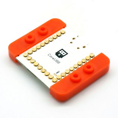
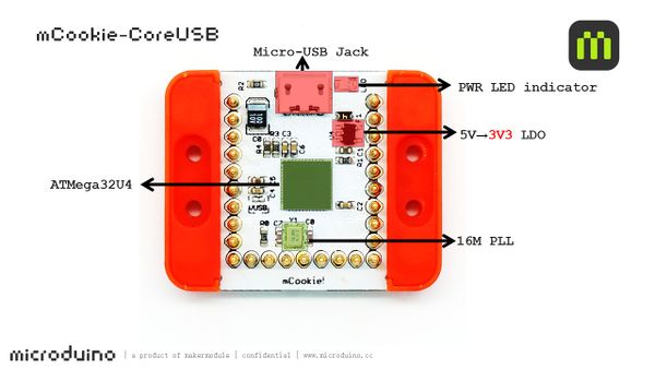
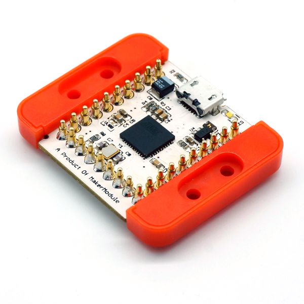
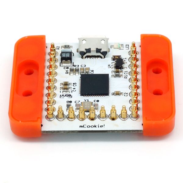
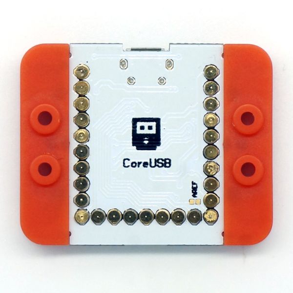
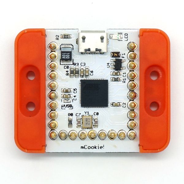
mCookie-CoreUSB is a 8-bit microcontroller development core board with ATMEGA32U4 series as the core, which is an open source, Arduino Leonardo compatible controller module.
mCookie adopts the same Java/C development environment with Arduino. Users can use Arduino IDE with other software Flash or Processing as well as mCookie and other electronic components, modules and sensors to make lots of interesting and interactive works.
Features
- Contain microcontroller and USB communication and enable to download programs via USB port.
- USB overcurrent protecton.
- Small, stackable, economic and open source.
- Open source hardware circuit design and Arduino compatible development environment for programming.
- Uniform mCookie interface standard makes it easy and flexible to connect with other mCookie modules and sensors.
Specification
| Flash |
32 KB (ATMEGA32U4))and 4KB of which are used for guide the program.
|
| SRAM |
2.5 KB (ATMEGA32U4)
|
| EEPROM |
1 KB (ATMEGA32U4)
|
| Clock Frequency0 |
16 MHz
|
- Twenty two digital I/O ports:
- Marked on the module as D0-D13 and A0-A7.
- Ten analog I/O ports:
- Marked on the module as A0,A1,A2,A3,A6,A7,D8(A8),D9(A9),D3(A10) and D4(A11).
- Each port provides a 10-bit resolution (0-1024). By default, the measuring range of voltage is the voltage values from GDN to VCC.
- For more information, please refer to: analogRead() .
- Support eight PWM output ports:
- Marked on the module as SCL,D3,D4,D5,D6,D7,D8 and D9.
- For more information, please refer to:analogWrite().
- Support two serial ports:
- USB analog Serial USB
- Marked as Serial1[D0(RX) and D1(TX)].
- Support SPI:
- Marked as D13(SCK),D12(MISO),D11(MOSI) and D10(SS).
- Support I2C:
- Marked as SDA(D18) and SCL(D19).
- External input:
- Marked as SCL(interrupt0),SDA(interrupt1),D0(interrupt2),D1(interrupt3) and D2(interrupt4).
- For more information, please refer to: attachInterrupt().
- Support ISP download.
| Pin
|
Original Pin Name
|
Map Pin Name
|
Digital Pin
|
Analog Pin
|
interrupt
|
PWM
|
Serial
|
SPI
|
I2C
|
Power
|
| 1 |
VCC |
+5V |
|
|
|
|
|
|
|
+5V
|
| 2 |
VCC |
+3V3 |
|
|
|
|
|
|
|
+3.3V
|
| 3 |
(OC0A/OC1C/#RTS)PB7 |
D7 |
D7 |
|
|
yes |
|
|
|
|
| 4 |
(OC1B/0C4B/ADC13)PB6 |
D8 |
D8 |
A8 |
|
yes |
|
|
|
|
| 5 |
(OC1A/#OC4B/ADC12)PB5 |
D9 |
D9 |
A9 |
|
yes |
|
|
|
|
| 6 |
(SS)PB0 |
D10 |
D10 |
|
|
|
|
SS |
|
|
| 7 |
(PDI/MOSI)PB2 |
D11 |
D11 |
|
|
|
|
MOSI |
|
|
| 8 |
(PDO/MISO)PB3 |
D12 |
D12 |
|
|
|
|
MISO |
|
|
| 9 |
(SCK)PB1 |
D13 |
D13 |
|
|
|
|
SCK |
|
|
| 10 |
AREF |
Exterior power |
|
|
|
|
|
|
|
|
| 11 |
(ADC7/TDI)PF7 |
A0 |
D14 |
A0 |
|
|
|
|
|
|
| 12 |
(ADC6/TDO)PF6 |
A1 |
D15 |
A1 |
|
|
|
|
|
|
| 13 |
(ADC5/TMS)PF5 |
A2 |
D16 |
A2 |
|
|
|
|
|
|
| 14 |
(ADC4/TCK)PF4 |
A3 |
D17 |
A3 |
|
|
|
|
|
|
| 15 |
(SDA/INT1)PD1 |
SDA |
D18 |
|
1 |
|
|
|
SDA |
|
| 16 |
(OC0B/SCL/INT0)PD0 |
SCL |
D19 |
|
0 |
yes |
|
|
SCL |
|
| 17 |
(ADC1)PF1 |
A6 |
D20 |
A6 |
|
|
|
|
|
|
| 18 |
(ADC0)PF0 |
A7 |
D21 |
A7 |
|
|
|
|
|
|
| 19 |
(RXD1/AIN1/INT2)PD2 |
D0 |
D0 |
|
2 |
|
1(RX) |
|
|
|
| 20 |
(TXD1/INT3)PD3 |
D1 |
D1 |
|
3 |
|
1(TX) |
|
|
|
| 21 |
(INT6/AIN0)PE6 |
D2 |
D2 |
|
4 |
|
|
|
|
|
| 22 |
(T1/#OC4D/ADC9)PD6 |
D3 |
D3 |
A10 |
|
yes |
|
|
|
|
| 23 |
(T0/OC4D/ADC10)PD7 |
D4 |
D4 |
A11 |
|
yes |
|
|
|
|
| 24 |
(OC3A/#OC4A)PC6 |
D5 |
D5 |
|
|
yes |
|
|
|
|
| 25 |
(ICP3/CLK0/OC4A)PC7 |
D6 |
D6 |
|
|
yes |
|
|
|
|
| 26 |
RESET |
RST |
|
|
|
|
|
|
|
|
| 27 |
GND |
GND |
|
|
|
|
|
|
|
GND
|
Document
Development
- Set development environment and install the drive as follows:
Projects
MCookie_(Microduino Compatible)Tutorial
FQA
Purchase
History
Microduino-CoreUSB
Pictures
Video
|
