Purpose
The tutorial talks about how Microduino D10 pin outputs PWM waveform and drive P-channel field-effect transistor, showing us the basic principle of Buck circuit.
Equipment
Microduino-Core is the 8-bit single-chip development core board with Atmel ATmega328P as the core, which is an open and Arduino Uno compatible controller.
Microduino-USBTTL is the program download module, capable of connecting with Microduino-Core or Microduino-Core+ and making the modules communicate with the computer. It uses MicUSB as the download interface, which is also the smallest part of Microduino. Microduino is just as small as a quarter. Besides, the download cable is just like the USB cable of most smart phones, easy to use.
| Related hardware |
Number |
Function
|
| Inductor 56uH 1A |
One |
Energy storage device in Buck circuit.
|
| Diode 1N5819 |
One |
For subsequent flow. (with higher work frequency than Diode 1N4007.)
|
| Capacitor 10uF 16V |
One |
Filter to output terminal.
|
| 100 Ω resistor |
Several |
Field-effect thyristor gate drive resistor as well as LED current limiting resistance.
|
| Field-effect transistor AO3401 |
One |
P-channel field-effect transistor.
|
| USB cable |
One |
For connecting Microduino modules and PC.
|
| Breadboard |
One |
For circuit buildup.
|
| Jumper |
One box |
Served as the connector.
|
Filed-effect Transistor
- Brief Introduction
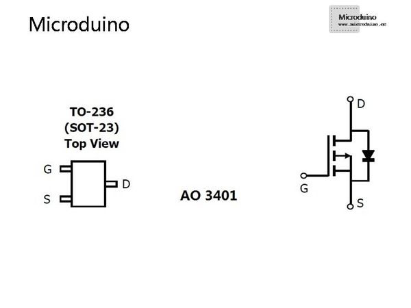
- Filed-effect transistor(FET) can be divided into two types-- N-channel and P-channel. The FET's three terminals are Source(S), Drain(D) and Gate(G). Here in this example, AO3401 belongs to P-channel field-effect transistor.
- Measurement
- When measuring the FET with a digital multimeter, you can tell the three terminals through the diode below. For P-channel EFT, when the reading of the multimeter is over 400 or 500, the black test pen connects to the terminal of S and the red pen to D. The pin without connecting to a test pen is G. For N-channel FET, however, the red pen connects to S and the black pen to D. If the reading is irregular, you can short the three pins and then measure so as to release storing charges of the Gate terminal. The most common FET damage is puncture shot when three pins seemingly get connected together, which is easy for the multimeter to measure.
You can check N-channel FET(AO3400) and P-channel(AO3401)’s PDF files below :
N-channel FET(AO3400) file download:File:AO3400.pdf
P-channel(AO3401) file download:File:AO3401.pdf
Buck Circuit
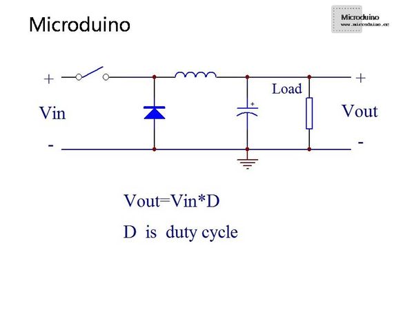
- Press the key(when the switch tube is unblocked), Vin inputs energy into inductance via the switch and meantime, part of the energy gets to the output end(load end).
- Disconnect the key(when the switch tube is blocked), the stored energy in inductance can be transmitted to the output end via the diode. At the this time, Vin doesn't supply energy to the load.
- With the capacitor, the output end can acquire direct current.
- Without considering the pressure drop of the diode, Vout=Vin*D(D stands for duty ratio). Eg. D =0.2 and Vin=12V, then the output voltage Vout=2.4V.
- Buck circuit belongs to switching power supply circuit and the switch tube works under nonlinear adjustment tube state, so it is more efficient than the linear adjustment power supply. In actual application, When the voltage of the PCB power supply is 24V or 12V, adopting Buck circuit is a good choice if you want to acquire 5V or 3.3V to supply MCU.
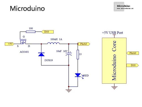
- Note: In this example, when D10 outputs high electrical level, the switch tube is under closing state. (Theoretical output voltage:Vout=Vin*(1-D). D=OCR1B/OCR1A. )
Schematic
Program
void setup()
{
  Serial.begin(9600);
  pinMode(10, OUTPUT);
  TCCR1A =_BV(COM1A0) | _BV(COM1B1) | _BV(WGM11) | _BV(WGM10);
  TCCR1B =_BV(WGM12) |_BV(WGM13) | _BV(CS10);
  OCR1A=400;//change this value to get diff period   OCR1A=400  F=40K
  OCR1B=300;//this value  need  modify to get diff duty cycle
}
void loop()
{
  int myAnaValue=analogRead(A0);
  float myAnaVol=myAnaValue/1023.0*5;
  Serial.println(myAnaVol);
  delay(1000);
}
Debugging
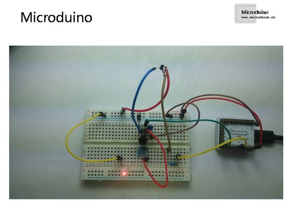
- Make sure the connection is all right.
- Copy the program to Arduino IDE.
- Compile the program and choose the right board as well as the related serial port.
- Click Upload and open the serial monitor of Arduino IDE after the upload and watch the data.
- Change the value of OCR1B, reprogram and then open the serial monitor and watch the data.
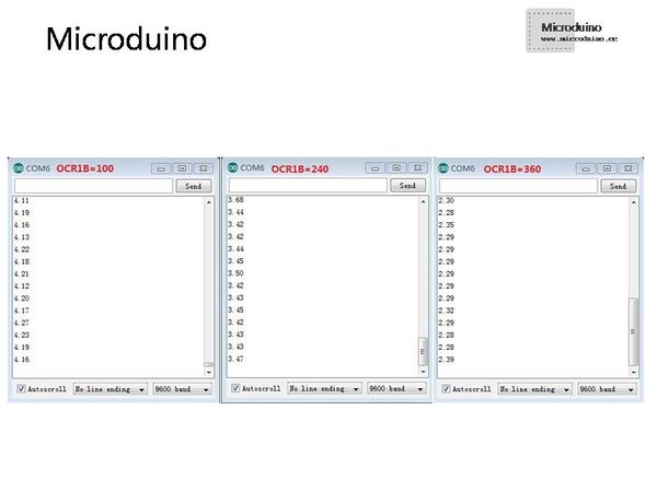
- Below is the data measured in real time, just for reference. (The value of OCR1A is 400.) Deviation between the actual output voltage and the theoretical value is a lot, because freewheeling diode exists pressure drop and the inductance and the load are inappropriate. When the duty ratio of Microduino's D10 pin changes, the change trend of the output voltage is reasonable.
Duty ratio
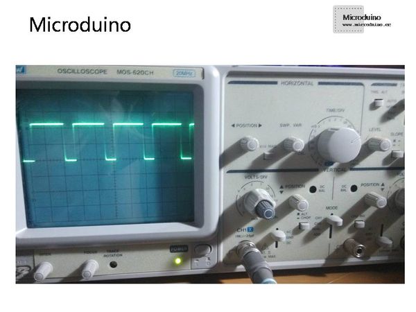
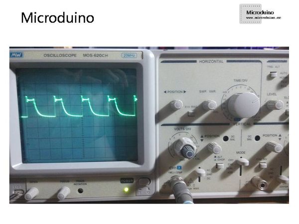
- Oscilloscope waveform measurement for reference.
D10 waveform OCR1B=300 OCR1A=400 10uS/div 2V/div
Remove the capacitor of the output terminal Waveform OCR1B=300 OCR1A=400 10uS/div 2V/div
Result
The Buck circuit an change output voltage value when changing duty ratio. The example is only suitable when Microduino's D10 pin outputs PWM rectangular wave, representing Buck circuit. In the actual application, you need to choose the right component parameters according to different load voltage and current as well as input voltage.
Video
|
