|
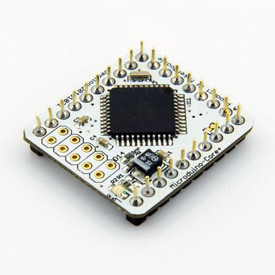
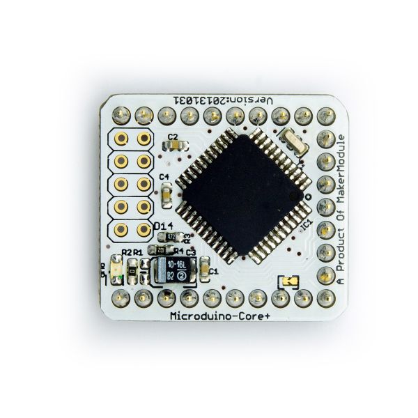
Microduino-Core+ is an 8-bit microcontroller development core board based on Atmel ATmega1284P and ATmega644PA series as the core and it is an open-source controller module compatible with Arduino UNO.
Beside Microduino-core+ has the features of Microduino-Core, the number of input and output of Flash, RAM, EEPROM of it has been greatly improved, and the pin conforms to the norms of Microduino, and the players can upgrade core to core+ smoothly, without modifying the arduino code basically.
Microduino uses java and C language development environment, same to Arduino. Players can use Arduino IDE, cooperated with software such as Flash or Processing , with Microduino and other electronic components, modules and sensors to make many funny interactive works.
Features
- Strong configuration. Its biggest Flash and SRAM can arrive 128KB and 16KB respectively.
- Small, cheap, stackable, and open.
- Open source hardware circuit design, and compatible-with Arduino programming development environment;
- Same with Arduino, Microduino can use ISP download line to program to 「bootloader」 flexibly;
- The unified Microduino interface specification and abundant peripheral modules can be connected and extended with other modules and sensors conformed to the Microduino interface specification conveniently and flexibly;
- 2.54 spacing mother of interface is convenient to integrate into the hole plate.
|
Specification
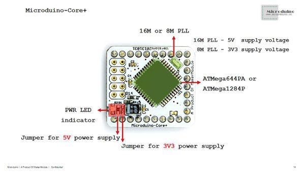
- Microduino-Core+According to the different core and clock frequency, there are four different versions at present:
| MCU type
|
Flash
|
SRAM
|
EEPROM
|
Clock frequency
|
Work voltage
|
| ATmega644PA
|
64K
|
4K
|
2K
|
16M
|
5.0V
|
| ATmega644PA
|
64K
|
4K
|
2K
|
8M
|
3.3V
|
| Atmega1284P
|
128K
|
16K
|
4K
|
16M
|
5.0V
|
| ATmega1284P
|
128K
|
16K
|
4K
|
8M
|
3.3V
|
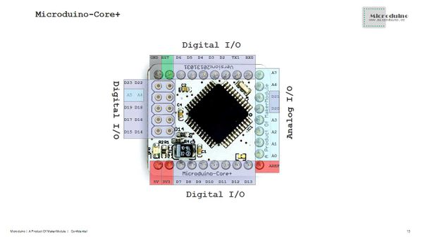
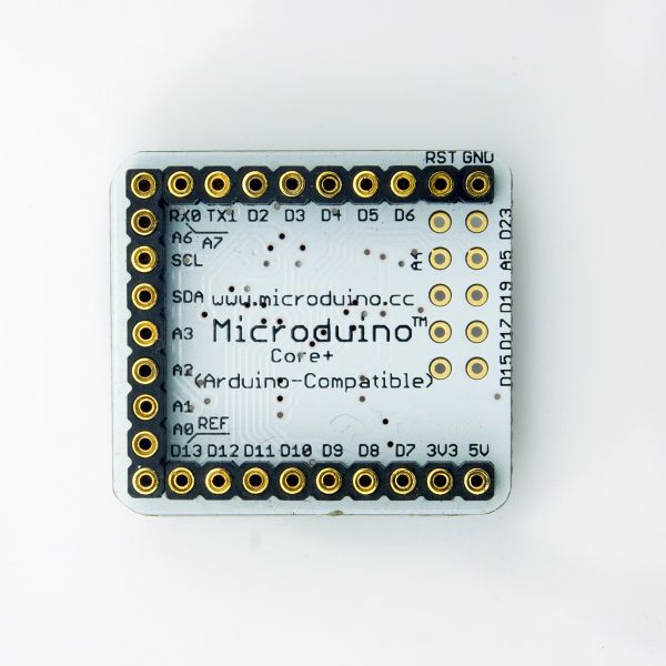
- Digital I/O There are 32 number digital input/output:
- Labeled on the module of D0, D1, D2~D13 and A0~A7, and the 10 (D14~D23) more than core .
- Analog I/O There are 8 analog input/output:
- Labeled on the module of A0~A7;
- Each provides a 10-bit resolution(that is 0~1024). By default, analog value measurement range is from GND to VCC voltage value;
- Please refer to analogRead() function.
- There are 8 PWM supports:
- Labeled on the module of respectively D7,D8,D9,D10,D12,D13,D22,D23.
- Please refer to analogWrite() function.
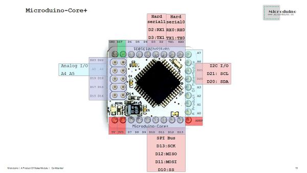
- There are two serial port supports:
- Labeled on the module of Serial[D0(RX),D1(TX)] and Serial1[D2(RX),D3(TX)].
- Connected with USBTTL,it will occupy D0 and D1. If the ports D0 and D1 are also occupied by other modules, this will lead to the communication with USBTTL is abnormal and the program can not be downloaded.
- There is one SPI support:
- Labeled on the module of D13(SCK),D12(MISO),D11(MOSI) and D10(SS).
- There is one 12C support:
- Labeled on the module of SDA(D20),SCL(D21).
- There are 3 external interrupt supports:
- Labeled on the module of D2(interrupt0),D3(interrupt1) and D6(interrupt2).
- Please refer toattachInterrupt()function.
- Support the ISP download function.
- Support the AREF end.
| Pin
|
Original Pin Name
|
Map Pin Name
|
Digital Pin
|
Analog Pin
|
interrupt
|
PWM
|
Serial
|
SPI
|
I2C
|
Power
|
| 1 |
VCC |
+5V |
|
|
|
|
|
|
|
+5V
|
| 2 |
VCC |
+3V3 |
|
|
|
|
|
|
|
+3.3V
|
| 3 |
(OC0A/AIN1)PB3 |
D7 |
D7 |
|
|
yes |
|
|
|
|
| 4 |
(OC2B/ICP)PD6 |
D8 |
D8 |
|
|
yes |
|
|
|
|
| 5 |
(OC1A)PD5 |
D9 |
D9 |
|
|
yes |
|
|
|
|
| 6 |
(OC0B/SS)PB4 |
D10 |
D10 |
|
|
yes |
|
SS |
|
|
| 7 |
(MOSI)PB5 |
D11 |
D11 |
|
|
|
|
MOSI |
|
|
| 8 |
(MISO)PB6 |
D12 |
D12 |
|
|
|
|
MISO |
|
|
| 9 |
(SCK)PB7 |
D13 |
D13 |
|
|
|
|
SCK |
|
|
| 10 |
AREF |
AREF |
|
|
|
|
|
|
|
|
| 11 |
(ADC7)PA7 |
A0 |
D24 |
A0 |
|
|
|
|
|
|
| 12 |
(ADC6)PA6 |
A1 |
D25 |
A1 |
|
|
|
|
|
|
| 13 |
(ADC5)PA5 |
A2 |
D26 |
A2 |
|
|
|
|
|
|
| 14 |
(ADC4)PA4 |
A3 |
D27 |
A3 |
|
|
|
|
|
|
| 15 |
(SDA)PC1 |
SDA |
D20 |
|
|
|
|
|
SDA |
|
| 16 |
(SCL)PC0 |
SCL |
D21 |
|
|
|
|
|
SCL |
|
| 17 |
(ADC1)PA1 |
A6 |
D30 |
A6 |
|
|
|
|
|
|
| 18 |
(ADC0)PA0 |
A7 |
D31 |
A7 |
|
|
|
|
|
|
| 19 |
(RXD0)PD0 |
D0 |
D0 |
|
|
|
0(RX) |
|
|
|
| 20 |
(TXD0)PD1 |
D1 |
D1 |
|
|
|
0(TX) |
|
|
|
| 21 |
(INT0)PD2 |
D2 |
D2 |
|
0 |
|
1(RX) |
|
|
|
| 22 |
(INT1)PD3 |
D3 |
D3 |
|
1 |
|
1(TX) |
|
|
|
| 23 |
(XCK0/T0)PB0 |
D4 |
D4 |
|
|
|
|
|
|
|
| 24 |
(CLKO/T1)PB1 |
D5 |
D5 |
|
|
|
|
|
|
|
| 25 |
(INT2/AIN0)PB2 |
D6 |
D6 |
|
2 |
|
|
|
|
|
| 26 |
RESET |
RST |
|
|
|
|
|
|
|
|
| 27 |
GND |
GND |
|
|
|
|
|
|
|
GND
|
| 28 |
(TOSC2)PC7 |
D14 |
D14 |
|
|
|
|
|
|
|
| 29 |
(TOSC1)PC6 |
D15 |
D15 |
|
|
|
|
|
|
|
| 30 |
(TDI)PC5 |
D16 |
D16 |
|
|
|
|
|
|
|
| 31 |
(TDO)PC4 |
D17 |
D17 |
|
|
|
|
|
|
|
| 32 |
(TMS)PC3 |
D18 |
D18 |
|
|
|
|
|
|
|
| 33 |
(TCK)PC2 |
D19 |
D19 |
|
|
|
|
|
|
|
| 34 |
(ADC3)PA3 |
A4 |
D28 |
A4 |
|
|
|
|
|
|
| 35 |
(ADC2)PA2 |
A5 |
D29 |
A5 |
|
|
|
|
|
|
| 36 |
(OC1B)PD4 |
D22 |
D22 |
|
|
yes |
|
|
|
|
| 37 |
(OC2A)PD7 |
D23 |
D23 |
|
|
yes |
|
|
|
|
|
Document
- The main components used in Microduino-core+ .
|
Development
- 1.Downloading programs to Microduino-core , players need to useMicroduino-USBTTL module.
- 2.The installation tutorial of the development environment and the driver environment is as following:
- Program Microduino BootLoader.
|
Application
|
FAQ
- Q:How do I judge that the voltage of the Core+ is 3.3V or 5V?
- A:Look at the resistor. If the R1 is welded, it is 3.3V. And if the R2 is welded, it is 5V.
- Q:Can I use 3.3V voltage to supply power to the Core+ of 16m clock frequency?
- A:It is not recommended . If the voltage is too low, it is easy to be unstable.
- Q:Can I use 5V voltage to supply power to the Core+ of 8M clock frequency?
Purchase
|
Map Storage
|
History
|
